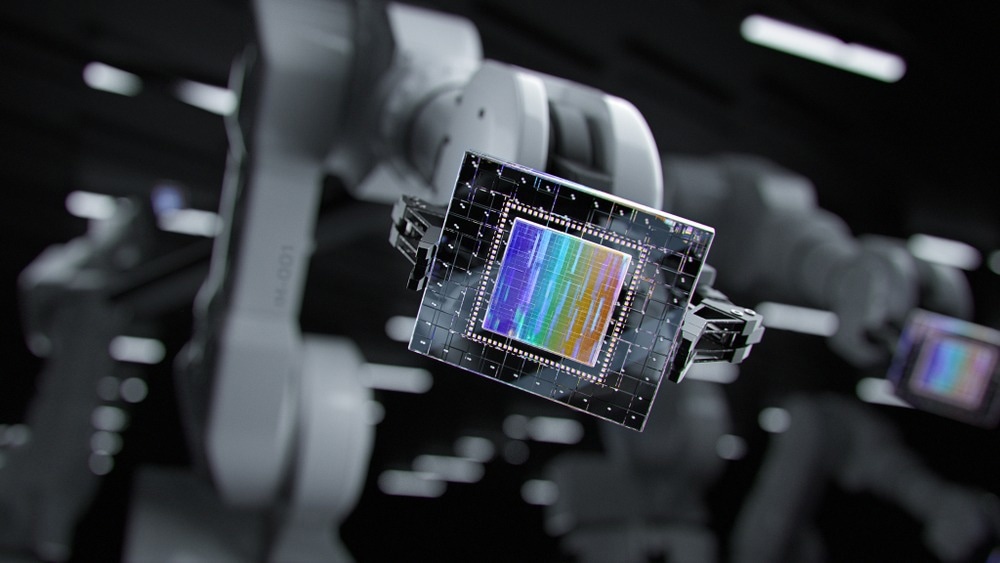
Semiconductor fabrication involves a series of highly precise processes that demand a high level of accuracy and repeatability to ensure the quality of the final products. Traditionally, these tasks were performed by skilled human operators, but the industry is now turning towards automation and robotics to meet this high level of precision and repeatability.

Image Credit: Gorodenkoff/Shutterstock.com
Semiconductor Fabrication Process
Semiconductor fabrication is a process central to manufacturing electronic components. The process starts with the fabrication of silicon wafers and uses photolithography to imprint complex circuit designs. Subsequent steps include deposition, etching, and doping to modify surface properties, forming transistors and other vital elements. Layers of insulating materials and metal interconnects are added, creating the intricate circuitry. This sequence transforms raw materials into advanced semiconductor devices, vital to countless electronic applications.
Advantages of using Robotics in Semiconductor Fabrication
Robotics provide high precision and accuracy in semiconductor fabrication since modern robots are equipped with advanced sensors and machine vision systems that execute tasks with micron-level accuracy, significantly reducing the margin of error in critical processes. This precision is crucial for manufacturing the smaller and more complex semiconductor components demanded by modern electronics.
Moreover, unlike human operators, robots do not need breaks, allowing for continuous, uninterrupted manufacturing processes that not only accelerate production timelines but also ensure a consistent level of quality throughout the fabrication process.
Some stages of semiconductor fabrication involve working with hazardous materials that may pose risks to human health. Robots can handle these materials, reducing the exposure of human operators to potentially harmful substances and enhancing safety in the manufacturing environment.
Commercial Landscape
Several companies are at the forefront of integrating robotics into semiconductor fabrication, showcasing the practical benefits of automation in improving manufacturing efficiency in real-world scenarios.
ASML's Robotic Lithography Systems
ASML, a leading supplier of photolithography equipment, has introduced robotic systems that play a pivotal role in improving semiconductor manufacturing efficiency. ASML employs cutting-edge robotic lithography systems in semiconductor fabrication, featuring magnetically levitating wafer tables that accelerate at impressive speeds of 7g without vibration or heating issues, enabling rapid loading, printing, and unloading of wafers up to 275 times per hour. The system's ability to synchronize wafer and reticle motion at nanometer and nanosecond levels, even at high accelerations, is crucial for producing functional microchips.
Fanuc's Robots
Fanuc, a pioneer in industrial robotics, has introduced collaborative robots (cobots) designed for tasks such as assembly and packaging in semiconductor manufacturing. These robots can work alongside human operators, streamlining the assembly line and increasing efficiency. For instance, Fanuc's M-20iB/25C is a highly efficient robot designed for the semiconductor industry due to its high precision and accuracy.
KUKA's Robotic Arm in Wafer Handling
KUKA, a global automation company, has developed robotic arms designed for wafer handling in semiconductor fabrication. KUKA's wafer handling solution is a mobile robotic system that consists of a standardized, automated guided vehicle (AGV), the LBR iiwa 14 R820 CR lightweight robot, a sophisticated wafer handling gripper, and certified software designed for automated material transportation in semiconductor production. This system offers precise, autonomous navigation with omnidirectional motion and laser scanners, ensuring efficient handling of 200mm and 300mm wafers. The LBR iiwa robot has vibration-free handling and earthquake protection in the gripper system.
Recent Development
A 2020 study addresses the challenges in semiconductor fabrication, focusing on robotic cluster tools used in wafer processing. Recent advancements in semiconductor materials, like carbon nanotubes and graphene, have led to narrower circuit line widths (less than ten nanometers).
The study introduces a novel approach to post-processing time-aware scheduling for robotic cluster tools, emphasizing the need for fast wafer removal to ensure high-quality integrated circuits and improved semiconductor fabrication efficiency. The proposed algorithms aim to optimize throughput and minimize post-processing time, considering wafer residency time constraints.
Challenges
There are some challenges associated with the integration of robotics in semiconductor fabrication. As manufacturing processes become more automated, there is a growing need for skilled technicians capable of programming, maintaining, and troubleshooting robotic systems.
Similarly, the upfront costs of implementing robotic solutions can be substantial, and companies must carefully weigh the initial investment against the long-term benefits. However, as technology advances and economies of scale come into play, the costs associated with robotics in semiconductor fabrication are likely to decrease, making automation more accessible to a broader range of manufacturers.
Conclusion
In conclusion, integrating robotics into semiconductor fabrication has proven to significantly enhance efficiency and safety in manufacturing processes. The precision and accuracy of modern robots equipped with advanced sensors and machine vision systems are crucial for meeting the demands of producing smaller, more intricate semiconductor components.
Companies like ASML, Fanuc, and KUKA showcase the practical benefits of automation with cutting-edge robotic systems tailored for semiconductor fabrication. Despite challenges such as the need for skilled technicians and upfront costs, ongoing technological advancements are expected to mitigate these concerns. The future holds promise for a more accessible and streamlined semiconductor manufacturing landscape through continued automation.
References and Further Reading
Lee, TE., Kim, HJ., Yu, TS. (2023). Semiconductor Manufacturing Automation. In: Nof, S.Y. (eds) Springer Handbook of Automation. Springer Handbooks. Springer, Cham. https://doi.org/10.1007/978-3-030-96729-1_38
Pillai, D. (2006). The future of semiconductor manufacturing. IEEE Robotics & Automation Magazine. https://doi.org/10.1109/MRA.2006.250560
Zhu, Q., Qiao, Y., Wu, N., & Hou, Y. (2020). Post-processing time-aware optimal scheduling of single robotic cluster tools. IEEE/CAA Journal of Automatica Sinica. https://doi.org/10.1109/JAS.2020.1003069
Cleanroomrobot FANUC M-20iB/25C, Fanuc. Retrieved on December 18, 2023 from https://www.fanuc.eu/ch/en/robots/robot-filter-page/m-20-series/m-20ib-25c
Khan, Taha. (2022, July 25). Keeping Semiconductor Manufacturing Clean with Robotics. AZoRobotics. Retrieved on December 18, 2023 from https://www.azorobotics.com/Article.aspx?ArticleID=497
Electronics Kuka Wafer Handling Solution. KUKA. Retrieved on December 18, 2023 from https://www.kuka.com/-/media/kuka-downloads/imported/87f2706ce77c4318877932fb36f6002d/wafer_handling_solution_en.pdf?
Mechanics & Mechatronics. ASML Retrieved on December 18, 2023 from https://www.asml.com/en/technology/lithography-principles/mechanics-and-mechatronics
Disclaimer: The views expressed here are those of the author expressed in their private capacity and do not necessarily represent the views of AZoM.com Limited T/A AZoNetwork the owner and operator of this website. This disclaimer forms part of the Terms and conditions of use of this website.